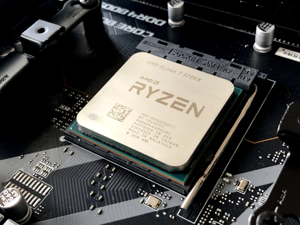
The relentless demand for data bandwidth in high-performance computing centers and AI GPU clusters has driven the PCI-SIG consortium to push physical interfaces to their limits. With the release of PCIe Gen 6 (PCI Express 6.0), the standard achieves an astonishing 64 GT/s per lane (up to 256 GB/s bidirectional bandwidth on a x16 slot), doubling the throughput of Gen 5.
However, achieving these speeds over copper traces required a complete overhaul of the physical layer (PHY), presenting massive signal integrity challenges for PCB layout designers.
The PAM4 Signaling Shift
For the first time in PCIe history, the standard abandons traditional Non-Return-to-Zero (NRZ) binary signaling in favor of PAM4 (Pulse Amplitude Modulation with 4 levels). While NRZ transmits 1 bit per clock cycle using two voltage states, PAM4 transmits 2 bits per cycle using four voltage levels (00, 01, 10, 11). This keeps the Nyquist frequency at a manageable 16 GHz, but reduces the eye height between voltage steps by a factor of three. Consequently, PAM4 is highly susceptible to noise and signal attenuation.
Forward Error Correction (FEC) and FLITs
Because the signal-to-noise ratio of PAM4 is significantly lower, PCIe Gen 6 introduces mandatory low-latency Forward Error Correction (FEC) to correct transmission bit errors on the fly. To make FEC computationally efficient, data packets are organized into fixed-sized FLITs (Flow Control Units) of 256 bytes. This structured packetization allows hardware decoders to detect and resolve errors with less than 2 nanoseconds of latency overhead, preserving the ultra-low latency requirements of memory-mapped PCIe operations.
Synapse Discussion
No approved comments yet. Be the first to share your thoughts!
Add private comment